Page 30 - EngineerIt July 2021
P. 30
ELECTRONICS


           Because inductance suppresses dynamic changes in current,   performance of LTC3310S, where an eight A load change results
        di/dt, when loads change, the current passing through this   in an output voltage excursion of less than ±40 mV, achieved with
        parasitic inductance is limited by its time constant, deteriorating   only 110 µF output capacitance.
        transient response. The result of parasitic inductance is voltage   Despite the obvious advantages of using high powered
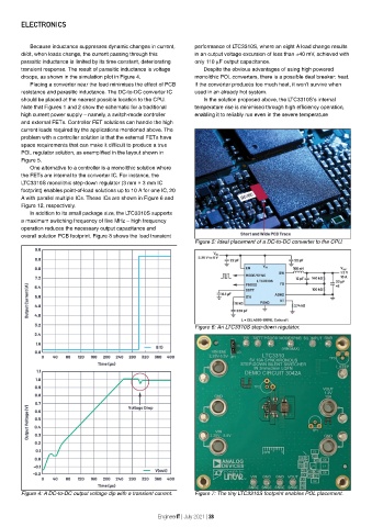
        droops, as shown in the simulation plot in Figure 4.   monolithic POL converters, there is a possible deal breaker: heat.
           Placing a converter near the load minimises the effect of PCB   If the converter produces too much heat, it won’t survive when
        resistance and parasitic inductance. The DC-to-DC converter IC   used in an already hot system.
        should be placed at the nearest possible location to the CPU.   In the solution proposed above, the LTC3310S’s internal
        Note that Figures 1 and 2 show the schematic for a traditional   temperature rise is minimised through high efficiency operation,
        high current power supply — namely, a switch-mode controller   enabling it to reliably run even in the severe temperature
        and external FETs. Controller FET solutions can handle the high
        current loads required by the applications mentioned above. The
        problem with a controller solution is that the external FETs have
        space requirements that can make it difficult to produce a true
        POL regulator solution, as exemplified in the layout shown in
        Figure 5.
           One alternative to a controller is a monolithic solution where
        the FETs are internal to the converter IC. For instance, the
        LTC3310S monolithic step-down regulator (3 mm × 3 mm IC
        footprint) enables point-of-load solutions up to 10 A for one IC, 20
        A with parallel multiple ICs. These ICs are shown in Figure 6 and
        Figure 12, respectively.
           In addition to its small package size, the LTC3310S supports
        a maximum switching frequency of five MHz — high frequency
        operation reduces the necessary output capacitance and
        overall solution PCB footprint. Figure 8 shows the load transient
                                                               Figure 5: Ideal placement of a DC-to-DC converter to the CPU.


                                                               Figure 6: An LTC3310S step-down regulator.


        Figure 4: A DC-to-DC output voltage dip with a transient current.  Figure 7: The tiny LTC3310S footprint enables POL placement.


                                                    EngineerIT | July 2021 | 28

