Page 23 - EngineerIT May 2022
P. 23
ELECTRONICS


           The level shifter circuit is large, creating a challenge for the   Challenge 2: Inefficiency
        designers. In addition, legacy negative DC-DC converter solutions   The legacy negative output DC-DC solution is inefficient. The
        are complex and inefficient, imposing yet another challenge.  extra heat generated due to inefficiency creates another
                                                               challenge for designers, who now have the extra burden of
        Challenge 1: level shifter                             removing that heat out of the system. Figure 5 is a simplified
        Figure 3 illustrates a typical level shifter circuit. Its purpose   circuit schematic of an example of such a system.
        is to shift the ground reference of a signal to match that of   This topology faces two inefficiency issues. First, it
        the system micro-controller. It is used here to translate the   employs non-synchronous switching where the output
        ON command from the system micro-controller to turn on/  rectifying diode, D1, dissipates more power compared to a
        off the DC-DC converter. This level shifter consists of nine   synchronous solution. Second, it has an extra power inductor,
        components. Its operation is straightforward: when ON is   L1, and an extra capacitor, C1, which also dissipates more
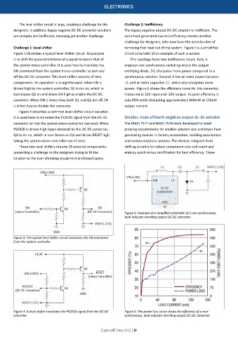
        driven high by the system controller, Q1 turns on, which in   power.  Figure 6 shows the efficiency curve for this converter,
        turn biases Q2 on and drives EN high to enable the DC-DC   measured at 12V input and -15V output. Its peak efficiency is
        converter. When ON is driven low, both Q1 and Q2 are off, EN   only 83% while dissipating approximately 460mW at 150mA
        is driven low to disable the converter.                output current.
           Figure 4 describes a common level-shifter circuit variation.
        It is used here to translate the PGOOD signal from the DC-DC   Smaller, more efficient negative output dc-dc solution
        converter so that the system micro-converter can read. When   The MAX17577 and MAX17578 were developed to meet
        PGOOD is driven high (open drained) by the DC-DC converter,   growing requirements for smaller-solution-size and lower-heat
        Q3 turns on, which in turn biases on Q4 and drives RESET high,   generating devices in factory automation, building automation,
        taking the system micro-controller out of reset.       and communications systems. The devices integrate level
           These two level shifters require 18 external components,   shifting circuitry to reduce component cost and count and
        presenting a challenge to the designers trying to fit the   employ synchronous rectification for best efficiency. These
        solution to the ever-shrinking equipment and board space.


                                                               Figure 5: Example of a simplified schematic of a non-synchronous,
                                                               dual-inductor inverting output DC-DC converter.


        Figure 3: The typical level shifter circuit translates the ON command
        from the system controller.


        Figure 4: A level shifter translates the PGOOD signal from the DC-DC   Figure 6: The power loss curve shows the efficiency of a non-
        converter.                                             synchronous, dual-inductor inverting output DC-DC converter.


                                                    EngineerIT | May 2022 | 21

