Page 20 - Issue 4 2023
P. 20
ELECTRONICS


                                                               step is to develop a product prototype that takes learnings
                                                               from the initial prototype work and integrates this into the
                                                               end solution. Part of this would be to modify the existing
                                                               schematics from the boards used, to remove the superfluous
                                                               items (test points, connectors, etc.). The user could then get
                                                               started on the PCB development, which would then show off
                                                               the importance and usability of the resources we provide with
                                                               each of our devices. For example, the optimised demo board
                                                               layout is a freely available resource provided for each of our
                                                               devices. While the demo board generally looks to be quite
                                                               large in size, this is simply to aid the testability and usability of
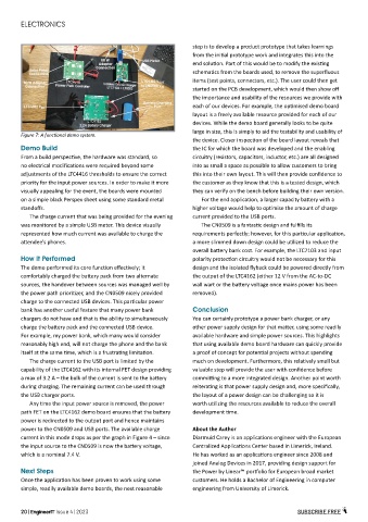
        Figure 7: A functional demo system.
                                                               the device. Closer inspection of the board layout reveals that
        Demo Build                                             the IC for which the board was developed and the enabling
        From a build perspective, the hardware was standard, so   circuitry (resistors, capacitors, inductor, etc.) are all designed
        no electrical modifications were required beyond some   into as small a space as possible to allow customers to bring
        adjustments of the LTC4416 thresholds to ensure the correct   this into their own layout. This will then provide confidence to
        priority for the input power sources. In order to make it more   the customer as they know that this is a tested design, which
        visually appealing for the event, the boards were mounted   they can verify on the bench before building their own version.
        on a simple black Perspex sheet using some standard metal   For the end application, a larger capacity battery with a
        standoffs.                                             higher voltage would help to optimise the amount of charge
           The charge current that was being provided for the evening   current provided to the USB ports.
        was monitored by a simple USB meter. This device visually   The CN0509 is a fantastic design and fulfills its
        represented how much current was available to charge the   requirements perfectly; however, for this particular application,
        attendee’s phones.                                     a more slimmed down design could be utilized to reduce the
                                                               overall battery bank cost. For example, the LTC7103 and input
        How It Performed                                       polarity protection circuitry would not be necessary for this
        The demo performed its core function effectively; it   design and the isolated flyback could be powered directly from
        comfortably charged the battery pack from two alternate   the output of the LTC4162 (either 12 V from the AC-to-DC
        sources, the handover between sources was managed well by   wall wart or the battery voltage once mains power has been
        the power path prioritizer, and the CN0509 nicely provided   removed).
        charge to the connected USB devices. This particular power
        bank has another useful feature that many power bank   Conclusion
        chargers do not have and that is the ability to simultaneously   You can certainly prototype a power bank charger, or any
        charge the battery pack and the connected USB device.   other power supply design for that matter, using some readily
        For example, my power bank, which many would consider   available hardware and simple power sources. This highlights
        reasonably high end, will not charge the phone and the bank   that using available demo board hardware can quickly provide
        itself at the same time, which is a frustrating limitation.  a proof of concept for potential projects without spending
           The charge current to the USB port is limited by the   much on development. Furthermore, this relatively small but
        capability of the LTC4162 with its internal FET design providing   valuable step will provide the user with confidence before
        a max of 3.2 A – the bulk of the current is sent to the battery   committing to a more integrated design. Another point worth
        during charging. The remaining current can be used through   reiterating is that power supply design and, more specifically,
        the USB charger ports.                                 the layout of a power design can be challenging so it is
           Any time the input power source is removed, the power   worth utilizing the resources available to reduce the overall
        path FET on the LTC4162 demo board ensures that the battery   development time.
        power is redirected to the output port and hence maintains
        power to the CN0509 and USB ports. The available charge   About the Author
        current in this mode drops as per the graph in Figure 4 – since   Diarmuid Carey is an applications engineer with the European
        the input source to the CN0509 is now the battery voltage,   Centralized Applications Center based in Limerick, Ireland.
        which is a nominal 7.4 V.                              He has worked as an applications engineer since 2008 and
                                                               joined Analog Devices in 2017, providing design support for
        Next Steps                                             the Power by Linear™ portfolio for European broad market
        Once the application has been proven to work using some   customers. He holds a Bachelor of Engineering in computer
        simple, readily available demo boards, the next reasonable   engineering from University of Limerick.


        20 | EngineerIT Issue 4 | 2023                                                           SUBSCRIBE FREE

