Page 13 - EngineerIT July 2022
P. 13
ELECTRONICS


        functions as the main switching circuitry   automatically controls the corresponding test and measurement equipment such as the
        of a buck (step-down) converter in   DC supply, electronic load, and multiplexed data acquisition device (DAQ) to measure
        conjunction with the LTC3861 dual,   temperature, current and voltage figures directly from the demo board, and then plot
        multiphase step-down voltage mode    those measurements on the GUI. Important telemetry data from on-board devices are also
                                                                             2
        DC-to-DC controller with accurate current   gathered by the software through PMBus/I C protocol. All this information is important in
        sharing.                             comparing system efficiency and power losses.

        DrMOS analysis evaluation            Data and results
        hardware                             The following test results cover the steady-state performance measurements, functional
        The analysis demonstration hardware has   performance waveforms, thermal measurement and output noise measurement. The
        the following key features:          demonstration board was tested with the following configurations:
        •  A PWM controller that can operate   •  Input voltage: 12 V
           on a wide range of input and output   •  Output voltage: 1 V
           voltages and switching frequencies.   •  Output load: 0 A to 60 A
           In this application, the controller is   •  Switching frequency: 500 kHz and 1 MHz
           LTC7883, a quad output polyphase
           step-down DC-to-DC voltage-mode
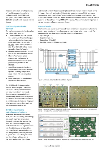
           controller, shown in Figure 2.
        •  Identical power stage design for both
           the LTC7051 and competitor devices.
        •  LTpowerPlay® power system
           management environment for
           comprehensive telemetry of system
           performance provided by the
           LTC7883.
        •  Can withstand extended ambient
           temperature in accordance with the
           specified operating temperature
           range of both ADI and competitor
           devices.
        •  Board is designed for easy thermal
           capture and measurement.          Figure 2. Analysis demonstration board block diagram.

        The DrMOS analysis demonstration
        board is shown in Figure 3. The board
        was carefully designed to include the
        key features previously mentioned.
        Components are symmetrically and
        systematically placed across each power
        rail and have the same PCB size and area
        to limit discrepancies between the power
        rails. Layout routing and layer stack-up
        are done symmetrically as well.

        DrMOS analysis testing               Figure 3. DrMOS evaluation board, top and bottom. PCB dimensions: 203 mm × 152 mm × 1.67
                                             mm (L × H × W) with 2 ounces of copper thickness.
        methodology and software
        Aside from the demonstration board
        itself, test setup and testing methodology
        are equally important for unbiased
        data and results. For this purpose, the
        team also created a complementary
        evaluation software with a graphical user
        interface (GUI) shown in Figure 4 for a
        more user-friendly approach of testing
        and data gathering. The user just needs
        to specify input and output parameters
        and the software will take care of
        the automated testing. The software   Figure 4. DrMOS evaluation software, showing the configuration and thermal analysis tab.


                                                    EngineerIT | July 2022 | 11

