Page 14 - EngineerIT July 2022
P. 14
ELECTRONICS


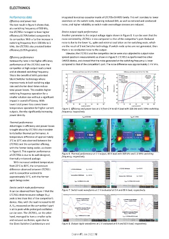
        Performance data                     integrated bootstrap capacitor inside of LTC705x DrMOS family. This will translate to lower
        Efficiency and power loss            overshoot on the switch node, meaning reduced EMI, as well as radiated and conducted
        The test result in figure 5 shows that,   noise, and higher reliability as switch-node overvoltage stresses are reduced.
        at a switching frequency of 500 kHz,
        the LTC7051 managed to have higher   Device output ripple performance
        efficiency (0.70% better) compared to   Another parameter is the output voltage ripple shown in Figure 8. It can be seen that the
        its competitor. With a further increase in   noise exhibited by LTC7051 is less compared to that of the competitor’s part. Reduced
        switching frequency from 500 kHz to 1   noise is due to the lower V DS spike and minimal oscillation on the switching node, which
        MHz, the LTC7051 also provided better   are the result of Silent Switcher technology. If switch-node spikes are not generated, then
        efficiency (0.95% greater).          there is no conducted noise to the output.
                                               Likewise, the LTC7051 and the competitor device were also subjected to output noise
        Efficiency performance               spread spectrum measurements as shown in Figure 9. LTC7051 outperformed the other
        Noteworthy here is the higher efficiency   DrMOS device, and showed that the noise generated at the switching frequency is lower
        performance of the LTC7051 over the   compared to that of the competitor’s part. The noise difference was approximately 1 mV rms.
        competitor at high output load current
        and at elevated switching frequency.
        This is the benefit of ADI’s patented
        Silent Switcher technology where
        improvements in both switching edge
        rate and shorter dead-times reduce
        total power losses. This enables higher
        switching frequency operation for a
        smaller solution size without a significant
        impact in overall efficiency. With
        lower total power loss comes lower
        temperature operation for higher current   Figure 5. Efficiency and power loss at 1 V from 0 A to 60 A load with 500 kHz and 1 MHz switching
        outputs, thereby significantly increasing   frequency, respectively.
        power density.

        Thermal performance
        Advantages in efficiency and power losses
        brought about by LTC7051 also translate
        to its better thermal performance. A
        temperature difference of approximately
        3°C to 10°C was observed between the
        LTC7051 and the competitor offering,
        with the former being cooler, as shown
        in Figure 6. This superior performance
        of LTC7051 is due to its well-designed,   Figure 6. Thermal performance at 1 V output, 60 A load with 500 kHz and 1.0 MHz switching
                                             frequency, respectively.
        thermally enhanced package.
           With increased ambient temperature
        from 25°C to 80°C, the temperature
        difference observed between LTC7051
        and its competitor widened to
        approximately 15°C, with the former
        again being cooler.

        Device switch node performance
        It can be observed from Figure 7 that the   Figure 7. Switch node waveforms at 1 V evaluated at 0 A and 60 A load, respectively.
        LTC7051 drain-to-source voltage (V DS)
        peak is less than that of the competitor’s
        device. Also, with the load increased to 60
        A, V DS measured on the competitor’s part
        is at its peak while prolonged oscillation
        can be seen. The LTC7051, on the other
        hand, managed to have a smaller spike
        and reduced oscillation, again due to
        the Silent Switcher 2 architecture and   Figure 8. Output ripple waveforms at 1 V evaluated at 0 A and 60 A load, respectively.


                                                    EngineerIT | July 2022 | 12

