Page 14 - Issue 3 2023
P. 14
INFRASTRUCTURE


        it can be difficult to achieve loop filter
        bandwidths above 2 MHz due to the
        small capacitor sizes required, and
        parasitic effects present at the PCB level
        disrupting the filter design. If an active
        loop filter is to be used, another rule
        of thumb is that the gain bandwidth
        product (GBP) of the op amp should be
        at least 10 times larger than the PFD
        frequency.
           Analog Devices’ free software
        ADIsimPLL™ can be used to perform
        frequency domain performance analysis
        and time domain ramp analysis of ADI
        PLLs that include ramp generators..
           The ADF4159 PLL includes ramp
        generation functionally and is included
        in the ADIsimPLL software, so this will
        be taken as our ramp generator for
        this example. Its maximum frequency
        of operation is 13 GHz so a VCO with a
        divide-by-2 output connected to the PLL
        input should be used to achieve a ramp
        covering the 24 GHz ISM band.

        Transmit (Tx) stage
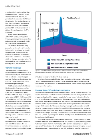
        To propagate the transmitted radar   Figure 2: A mock diagram of multiple detected radar targets and how the ramp bandwidth and
        signal efficiently by supplying the FMCW   phase noise affect the ability to detect and differentiate between each of the targets.
        ramp with enough gain and to interface
        with an antenna, a transmit stage is   (MIMO) operation (see the Other Features section).
        required. We have previously noted that   An LO signal is also required for the down conversion of the received radar signal.
        the radar’s range is a function of the   This LO frequency should be at the exact same frequency as the transmitted signal at
        transmitted signal’s strength.       each moment. For more details on the down conversion, see the receive stage (Rx) and
           A VCO is also required to lock to the   down conversion section.
        PLL discussed in the previous section.
        The transmit stage can be built discretely,   Receive stage (Rx) and down conversion.
        a VCO with its output split to the PLL   We have previously noted that to triangulate a target’s angular position, more than one
        feedback and to a PA stage. An integrated   receive channel is required. We have also seen that the accuracy in angle offset in which
        option is the ADF5901 MMIC transmit IC.   a target can be placed (the angular resolution) of a radar system is directly related to
        It has a 24 GHz to 24.25 GHz VCO with an   the number of receive channels it has. For the receive stage of our proposed radar, we
        in-built divide-by-2 output that pairs with   will consider the ADF5904 receive MMIC. The ADF5904 has four receive channels giving
        the choice of ADF4159 PLL. The ADF5901   relatively modest angular resolution. One way of increasing the number of channels is
        also includes a power amplifier (PA) at   using multiple receive ICs. This can be done by ensuring they all receive the same LO
        its output that gives up to 8 dBm output   signal for accurate down conversion. For two ADF5904 ICs, a passive splitter such as a
        power. This is sufficient for ranges up to   Wilkinson divider is sufficient, given the ADF5901 LO output power that is available and
        around 100 m (for RCS = 1 m2). To extend   the ADF5904’s LO input sensitivity. For a further increase of receive channels with more
        the range further, additional external PA   than two ADF5904 ICs, some gain in the form of a PA (such as the HMC863ALC4) would
        stages may be used.                  be required at the LO output.
           The ADF5901 has two transmit        While larger numbers of receive channels will result in a higher performance radar,
        output channels. For normal operation,   this does come with increased data loads – in turn, demanding more processing power.
        only one of these is used. The two   With many receive channels in an imaging radar, real-time processing could require an
        transmit channels can be alternated for   expensive FPGA solution with complex firmware routines, whereas limiting the number
        advanced multiple input multiple output   of channels means a comparatively low cost DSP can be used to perform processing


        14 | EngineerIT Issue 2 | 2023                                                     SUBSCRIBE FREE

