Page 18 - EngineerIt August 2021
P. 18
ICT 5G


        LNA to shunt any returned transmit power to a termination instead   Power
        of the core amplifier input. These various signals can be generated   Rolling up the total power dissipation is determined by many
        and orchestrated by the ASIC, FPGA or transceiver.     factors, including the FPGA selected and the functions
           The receiver signal chain includes a function that   implemented, the transceiver selected and options enabled, the
        correspondingly changes the digital data stream to account for   clock tree required, and the RF power generated.
        the reduced analogue gain, preserving the absolute signal level   A typical mid-range FPGA SoC implementing the O-RAN
        as it is passed to the low-PHY and then on to the remainder of the   CUS- and M-plane processing, along with synchronisation with
        baseband downstream.                                   IEEE 1588 v2 PTP stack, will consume around 15 W. The typical
           The application shown here is for single band. While the   ADRV9029 transceiver will dissipate between five and eight W,
        transceiver is broadband and covers all frequencies up to six GHz,   depending on TDD or FDD configuration along with the range of
        not all devices in the design do. Devices like the LNA and PA are   DFE functionality enabled. To this the clocking power, receiver
        typically banded and require selection based on band supported.   power, transmitter power, as well as miscellaneous powers must be
        Typically, these devices are available in pin-compatible options   added. Table 2 shows an example rollup of the total power for the
        to cover all common bands below six GHz and are easy to swap   system exclusive of the transmitter chain, which varies greatly with
        out. This enables support for all the popular TDD and FDD bands,   power output class.
        including those for 5G and those proposed for O-RAN.      Rolling up the power dissipation for the radio, total dissipation
                                                               for a 70:30 duty cycle for Tx:Rx shows 26 W to 29 W, depending
        Clock tree                                             on the exact radio configuration, excluding power associated with
        Depending on the configuration, several different clock   the PA. Table 3 shows a few examples of PA dissipation. Because
        configurations are possible. If precise timing alignment is required,   PAs operate largely in the linear range of the transistors in some
        then a two stage clock synthesis will be required. The first stage   variation of a class AB, their efficiency could be anywhere between
        will require linkage to the baseband by way of an ASIC, FPGA,   20% and 50%. This is where the value of integrated DPD is a big
        or controller to properly time and align the radio digitisation. This   benefit. Even for small bandwidth, low power PAs, a few dozen
        application will require processing of the precision time protocol   mW of DPD dissipation is more than offset by the improvement in
        (PTP) information provided by way of the fronthaul or by a local   efficiency of the PA.
        GPS receiver. This will ensure that the radio and baseband   For a low power small cell, adding in about 2.5 W of additional
        processor know precisely when radio frames should be processed.  power brings the total dissipation to about 30 W, which is comfortable
           The AD9545 family is ideally suited for precisely adjusting the   for a passively cooled indoor small cell powered by a PoE solution.
        frequency, phase and time of the main clock to the radio. It has the
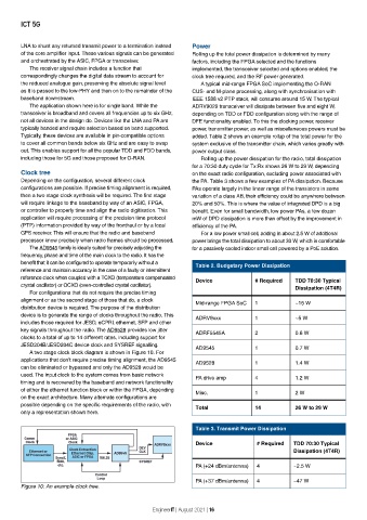
        benefit that it can be configured to operate temporarily without a   Table 2. Budgetary Power Dissipation
        reference and maintain accuracy in the case of a faulty or intermittent
        reference clock when coupled with a TCXO (temperature compensated   Device   # Required   TDD 70:30 Typical
        crystal oscillator) or OCXO (oven-controlled crystal oscillator).                        Dissipation (4T4R)
           For configurations that do not require the precise timing
        alignment or as the second stage of those that do, a clock   Mid-range FPGA SoC   1      ~15 W
        distribution device is required. The purpose of the distribution
        device is to generate the range of clocks throughout the radio. This   ADRV9xxx   1      ~5 W
        includes those required for JESD, eCPRI, ethernet, SFP and other
        key signals throughout the radio. The AD9528 provides low jitter   ADRF5545A   2         0.6 W
        clocks to a total of up to 14 different rates, including support for
        JESD204B/JESD204C device clock and SYSREF signalling.   AD9545              1            0.7 W
           A two stage clock block diagram is shown in Figure 10. For
        applications that don’t require precise timing alignment, the AD9545   AD9528   1        1.4 W
        can be eliminated or bypassed and only the AD9528 would be
        used. The input clock to the system comes from basic network   PA drive amp   4          1.2 W
        timing and is recovered by the baseband and network functionality
        of either the ethernet function block or within the FPGA, depending   Misc.   1          2 W
        on the exact architecture. Many alternate configurations are
        possible depending on the specific requirements of the radio, with   Total   14          26 W to 29 W
        only a representation shown here.

                                                                Table 3. Transmit Power Dissipation

                                                                Device              # Required   TDD 70:30 Typical
                                                                                                Dissipation (4T4R)

                                                                PA (+24 dBm/antenna)   4        ~2.5 W

                                                                PA (+37 dBm/antenna)   4        ~47 W
        Figure 10: An example clock tree.


                                                   EngineerIT | August 2021 | 16

