Page 14 - EngineerIt August 2021
P. 14
ICT 5G


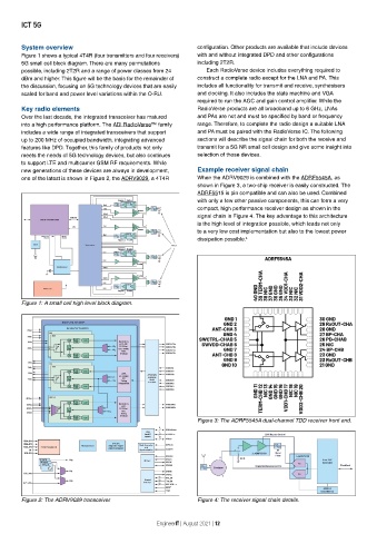
        System overview                                        configuration. Other products are available that include devices
        Figure 1 shows a typical 4T4R (four transmitters and four receivers)   with and without integrated DPD and other configurations
        5G small cell block diagram. There are many permutations   including 2T2R.
        possible, including 2T2R and a range of power classes from 24   Each RadioVerse device includes everything required to
        dBm and higher. This figure will be the basis for the remainder of   construct a complete radio except for the LNA and PA. This
        the discussion, focusing on 5G technology devices that are easily   includes all functionality for transmit and receive, synthesisers
        scaled for band and power level variations within the O-RU.  and clocking. It also includes the state machine and VGA
                                                               required to run the AGC and gain control amplifier. While the
        Key radio elements                                     RadioVerse products are all broadband up to 6 GHz, LNAs
        Over the last decade, the integrated transceiver has matured   and PAs are not and must be specified by band or frequency
        into a high performance platform. The ADI RadioVerse™ family   range. Therefore, to complete the radio design a suitable LNA
        includes a wide range of integrated transceivers that support   and PA must be paired with the RadioVerse IC. The following
        up to 200 MHz of occupied bandwidth, integrating advanced   sections will describe the signal chain for both the receive and
        features like DPD. Together, this family of products not only   transmit for a 5G NR small cell design and give some insight into
        meets the needs of 5G technology devices, but also continues   selection of those devices.
        to support LTE and multicarrier GSM RF requirements. While
        new generations of these devices are always in development,   Example receiver signal chain
        one of the latest is shown in Figure 2, the ADRV9029, a 4T4R   When the ADRV9029 is combined with the ADRF5545A, as
                                                               shown in Figure 3, a two-chip receiver is easily constructed. The
                                                               ADRF5515 is pin compatible and can also be used. Combined
                                                               with only a few other passive components, this can form a very
                                                               compact, high performance receiver design as shown in the
                                                               signal chain in Figure 4. The key advantage to this architecture
                                                               is the high level of integration possible, which leads not only
                                                               to a very low cost implementation but also to the lowest power
                                                               dissipation possible. 4


        Figure 1: A small cell high level block diagram.


                                                               Figure 3: The ADRF5545A dual-channel TDD receiver front end.


        Figure 2: The ADRV9029 transceiver.                    Figure 4: The receiver signal chain details.


                                                   EngineerIT | August 2021 | 12

