
Page 15 - EngineerIt August 2021
P. 15
ICT 5G
The architecture of the RadioVerse family leads to the
elimination of many elements typically associated with a classic
receiver design, including some of the RF amplification, filtering
and integration of much of the remaining radio functionality,
including channel filters (analogue and digital) and baseband
amplifiers. These are typically some of the largest and highest
power devices in the system, which results in significant savings
over other architectures like direct RF sampling.
As shown in Figure 4, the small cell receiver line-up consists
of a circulator (for TDD applications), ADRF5545A, SAW/BAW
(surface acoustic wave/bulk acoustic wave) or mono-block filter,
balun and transceiver. Additional amplifiers or VGAs are not
required given the good noise performance and low input IP1dB of
the ADRV9029 and other members of the RadioVerse family. Using
this signal chain, it is possible to support noise figures as low as
2 dB for the complete system from the antenna to bits. While this
design includes an integrated RF front-end module (FEM), many
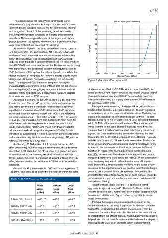
designs will still benefit from a discrete design not represented Figure 5: Receiver NF vs. input level.
here. The integrated FEM trades off integration for slightly
increased filter requirements in the antenna filter, but still offers a
compelling design for many highly integrated solutions such as of interest at an offset of ±7.5 MHz with no more than 6 dB de-
massive MIMO and other TDD deployments. Typically, discrete sense allowed. From Figure 5 showing the Analog Devices’ signal
front ends are used for FDD designs. chain performance, only about 0.9 dB de-sense has occurred.
Assuming a loss prior to the LNA of about 0.5 dB, and if the Narrow-band blocking is a slightly lower power CW-like stimulus
loss of the band filter is 1 dB, given the data sheet specs of the but is not a problem either.
two active devices, the nominal NF for the complete receiver Perhaps a more interesting challenge will be the out-of-band
signal chain should be about 2 dB. Assuming a 0 dB signal-to- blocking from section 7.5.2. Here a signal of –15 dBm is passed
noise-and-distortion ratio consistent with MCS-4, the reference to the antenna input. For a small cell with less than 200 MHz, the
sensitivity will be about –104.3 dBm for a G-FR1-A1-1 5G carrier closest this signal can be to the band edge is 20 MHz. The test
(~5 MHz). This should be more than adequate to meet even the requires a sweep from 1 MHz up to 12.75 GHz, excluding the band
wide area conducted requirements shown in section 7.2.2 of within 20 MHz of the operational frequency. There are several
38.104 with room for margin, and much more than enough for things working to the signal chain’s advantage here. First, the
a local area/small cell design that requires –93.7 dBm for this circulator has a finite bandwidth and will reject many out-of-band
condition as summarised in Table 1. Some low performance small signals, but close in it is not a big contributor. Second, the filter
cell applications may be able to utilise a single stage LNA such as shown after the ADRF5545A will provide some filtering — typically,
GRF2093 followed by a SAW filter. 20 MHz out-of-band ~20 dB rejection is reasonable. Finally, one
Additionally, 38.104 section 7.4.1 requires that under –52 of the unique and most useful features of ADI’s transceiver family,
dBm (wide area) ACS blocking, the receiver should not de-sense inherent to the transceiver architecture, is built-in out-of-band
more than 6 dB. Based on the NF vs. input level shown in Figure rejection. In Figure 20 from Analog Devices’ application note
5, very little additional noise occurs at –52 dBm than at lower AN-1354, inherent out-of-band rejection is demonstrated as an
levels. In fact, the noise floor doesn’t tilt upward until just after –40 increasing signal level to de-sense the receiver. In this application
dBm, which is ideal for the local area ACS that requires –44 dBm note, sweeping frequency in either direction around the pass
tolerance. band shows that a larger signal is tolerated for the same level of
General blocking requirements (7.4.2) call for an aggressor of de-sense. In the application note, we see that near the band edge
–35 dBm (local area) to be applied to the receiver within the band about 10 dB is possible for six dB de-sense. Beyond this, the
integrated filter rolls off significantly out-of-band signals, which do
Table 1. 38.104 Receiver Classifications not alias back in-band and are largely attenuated both by on-chip
and external filtering.
Wide Medium Local Together these blocks filter the –15 dBm out-of-band
Area Range Area aggressor to approximately –40 dBm to –45 dBm up to the
(dBm) (dBm) (dBm) 20 MHz exclusion band. Further out, even greater rejection would
be assumed. At this level, Figure 5 shows very little de-sense
5 MHz BW/15 kHz –101.7 –96.7 –93.7 would be expected.
Perhaps the bigger problem would be the linearity of the
20 MHz BW/15 kHz –95.3 –90.3 –87.3 front-end module. At this level, a significant IM3 product could be
anticipated. Depending on the actual FEM selected, it may be
50 MHz BW/30 kHz –95.6 –90.6 –87.6 desirable to move the band selection filter before the second LNA
to protect it from out-of-band signals, which typically produce large
100 MHz BW/30 kHz –95.6 –90.6 –87.6 IM products. It is not possible to place a filter between the stages on
these types of FEMs, so an alternate option is implemented.
EngineerIT | August 2021 | 13