Page 28 - EngineerIT November 2021
P. 28
AUTOMATION AND CONTROL


        constant current source for providing IEPE sensor supply current,   For multichannel DAQ systems that do not require channel
        an ADA4610-1 precision JFET buffer amplifier, an ADA4945-1 fully   isolation, the quad (AD7768-4) or octal (AD7768) version of the same
        differential amplifier for ADC driving and the construction of an anti-  ADC can be used.
        aliasing filter. An ADR444 precision reference source is used to provide
        the reference to the ADC with the help of an ADA4528-1 precision op   AFE design
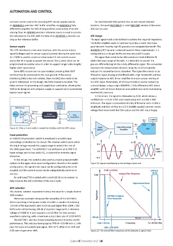
        amp as the reference buffer.                           The input signal needs to be buffered to achieve the required impedance.
                                                               The buffer amplifier needs to have low input bias current, low noise,
        Sensor supply                                          good dynamic linearity, high DC precision and adequate bandwidth. The
        The IEPE interface is a two-wire interface, with the sensor output   ADA4610-1 JFET op amp is selected based on these requirements. It is
        signal (voltage) and the sensor supply (current) sharing the same wire.   configured as a unity-gain buffer and requires a ±15 V supply.
        An LT3092 is used to construct a low noise 2.5 mA current source   The signal then needs to be attenuated and level shifted to fit
        across the 30 V supply to power the sensor. The current value can be   within the input range of the ADC. It is desirable to convert the
        programmed via resistor value in order to support longer cable length/  pseudo differential signal into a fully differential signal. This conversion
        higher cable capacitance.                              improves the measurement dynamic range by six dB and greatly
           Some IEPE sensors are not case-isolated, meaning their OUT   reduces the second harmonic distortion. The signal then needs to be
        terminal may be connected to the local ground. If the sensor   filtered to reject aliasing and buffered with a high bandwidth and low
        interfacing DAQ is also not isolated, then the DAQ also needs to be   output impedance ADC driver amplifier to ensure proper settling of
        ground referenced. In this design, the DAQ channel is isolated. This   the ADC input. Fortunately, all of these functions can be realised by
        helps remove the grounding and supply level constraints, allowing the   a circuit design using a single ADA4945-1 fully differential ADC driver
        DAQ to be designed with a bipolar supply to support more symmetrical   amplifier with minimum distortion and added noise while maintaining
        bipolar input signals.                                 excellent DC precision.
                                                                  In this circuit, the signal is attenuated by 0.33, which allows a
                                                               ±4.096/0.33 = ±12.41 V full-scale input swing with a 4.096 V ADC
                                                               reference. The signal is converted into fully differential with ±4.096 V
                                                               amplitude and level shifted to a 2.5 V (middle supply) common-mode
                                                               voltage that makes both the FDA output and the ADC input happy.


        Figure 11: Only a 2-wire cable is needed to interface with the IEPE sensor.

        Input protection
        An ADG5421F protection switch is employed to provide input
        overvoltage protection to the circuit. The internal switch opens when
        the input voltage exceeds the supply range to protect the rest of
        the DAQ signal chain. The ADG5421F can withstand up to ±60 V of
        input voltage and its low, stable R ON is essential to minimise signal
        distortion.
           In this design, this switch is also used to provide programmable
        options to the signal chain input configuration. Based on the switch   Figure 12: Signal conditioning in the analogue front end.
        configuration, the signal chain input can be configured as AC or DC
        coupled, and the current source can be independently switched in
        and out.
           An additional TVS is added with a small (10 Ω) series resistor to
        help improve the ESD protection of the input node.

        ADC selection
        The channel isolation requirement drives the need for a single-channel
        DAQ solution.
           These two examples showcase the versatility of the AD7768-1.
        When operating in full power mode, this ADC is capable of achieving
        110 kHz of flat bandwidth with the brick wall digital filter (ODR = 256
        kSPS) while still achieving 108 dB of dynamic range (with a reference
        voltage of 4.096 V). It also supports a sinc5 filter for time domain
        waveform capturing, with a maximum output data rate of 1.024 MSPS.
           The AD7768-1 also has industry-leading dynamic linearity and DC
        performance. This includes having typical THD of –120 dB with a 1 kHz
        near full-scale sinusoidal input signal, 300 nV/°C offset error drift and
        0.25 ppm of gain error drift.                          Figure 13: The overall filter responses of the Example 2 signal chain.


                                                 EngineerIT | November 2021 | 26

