Page 11 - EngineerIT November 2022
P. 11
ELECTRONICS DESIGN


                                                              Chopping artifacts 1-3,5-7
                                                              Although chopping works well to remove unwanted offset, drift
                                                              and 1/f noise, it produces unwanted AC artifacts such as output
                                                              ripple and glitches. Analog Devices’ recent zero-drift products
                                                              have taken steps to make the magnitude of these artifacts smaller
                                                              and located at higher frequencies, which makes filtering easier at
                                                              the system level.

                                                              Ripple Artifact
                                                              Ripple is a basic consequence of the chopping modulation
                                                              technique that moves these low frequency errors to odd
                                                              harmonics of the chopping frequency. Amplifier designers employ
        Figure 3: A basic auto-zero amplifier.
                                                              many methods to reduce the effects of ripple, including:
        input offset voltage and noise. Note that the amplifier is   •  Production offset trimming: The nominal offset can be
        unavailable for signal amplification during this phase. For an   significantly reduced by performing a one-time initial trim, but
        auto-zeroed amplifier to operate in a continuous manner,   the offset drift and 1/f noise remain.
        two identical channels must be interleaved. This is called   •  Combining chopping and auto-zeroing: The amplifier is first
        ping-pong auto-zeroing.                                  auto-zeroed, then chopped to upmodulate the increased noise
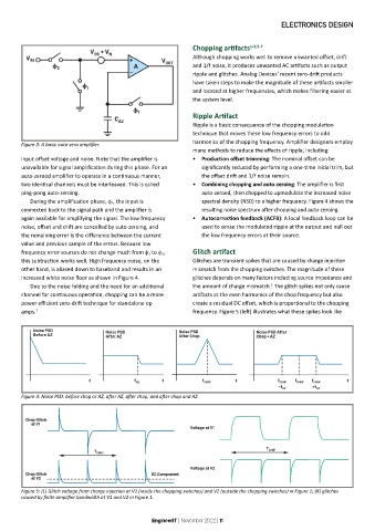
           During the amplification phase, ϕ 2, the input is     spectral density (NSD) to a higher frequency. Figure 4 shows the
        connected back to the signal path and the amplifier is   resulting noise spectrum after chopping and auto-zeroing.
        again available for amplifying the signal. The low frequency   •  Autocorrection feedback (ACFB): A local feedback loop can be
        noise, offset and drift are cancelled by auto-zeroing, and   used to sense the modulated ripple at the output and null out
        the remaining error is the difference between the current   the low frequency errors at their source.
        value and previous sample of the errors. Because low
        frequency error sources do not change much from ϕ 1 to ϕ 2,   Glitch artifact
        this subtraction works well. High frequency noise, on the   Glitches are transient spikes that are caused by charge injection
        other hand, is aliased down to baseband and results in an   mismatch from the chopping switches. The magnitude of these
        increased white noise floor as shown in Figure 4.     glitches depends on many factors including source impedance and
                                                                                       1
           Due to the noise folding and the need for an additional   the amount of charge mismatch.  The glitch spikes not only cause
        channel for continuous operation, chopping can be a more   artifacts at the even harmonics of the chop frequency but also
        power efficient zero-drift technique for standalone op   create a residual DC offset, which is proportional to the chopping
        amps. 2                                               frequency. Figure 5 (left) illustrates what these spikes look like


        Figure 4: Noise PSD: before chop or AZ, after AZ, after chop, and after chop and AZ.


        Figure 5: (L) Glitch voltage from charge injection at V1 (inside the chopping switches) and V2 (outside the chopping switches) in Figure 1; (R) glitches
        caused by finite amplifier bandwidth at V1 and V2 in Figure 1.


                                                 EngineerIT | November 2022 | 11

