Page 13 - EngineerIT November 2022
P. 13
ELECTRONICS DESIGN


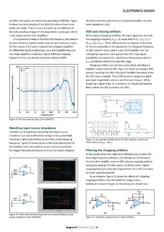
        an offset and ripple correction loop operating at 800 kHz. Figure   should ensure that each input of a chopped amplifier sees the
        9 shows the noise density of the ADA4522 where these noise   same impedance (top).
        peaks are visible. There is also a noise bump at 6 MHz due to
        the reduced phase margin of the loop when in unity gain, which   IMD and aliasing artifacts
        is not unique to zero-drift amplifiers.                When using a chopping amplifier, the input signal can mix with
           It is important to keep in mind that the frequency described in   the chopping frequency, f CHOP, to create IMD at f IN ± f CHOP, f IN ±
        the data sheet is a typical number and can vary from part to part.   2f CHOP, 2f IN ± f CHOP.  These IMD products can appear in the band
        For this reason, if the system requires two chopped amplifiers   of interest especially as fIN approaches the chopping frequency.
        for differential signal conditioning, use a dual amplifier because   To eliminate this issue, select a zero-drift amplifier that has
        two single amplifiers could have slightly different chopping   a chopping frequency much greater than the input signal
        frequencies that can interact and cause additional IMD.  bandwidth and ensure that interferers at frequencies close to
                                                               f CHOP are filtered before this amplifier stage.
                                                                  Chopping artifacts can also be aliased when sampling an
                                                               amplifier output with an ADC. Figure 11 shows an example IMD
                                                               product resulting from the aliasing of the glitch frequency when
                                                               the ADC takes a sample. These IMD products depend on glitch
                                                               and ripple magnitudes and can vary from part to part. When
                                                               designing a signal chain, it is necessary to include anti-aliasing
                                                               filters before the ADC to reduce this IMD.


        Figure 9: The noise density plot of the ADA4522.

        Matching input source impedance
        Transient current glitches interacting with input source
        impedance can cause differential voltage errors, potentially
        resulting in additional artifacts at multiples of the chopping   Figure 11: An example of IMD where the ADC samples a glitch and
        frequency. Figure 10 shows spikes in the noise density plot of   causes alias at f SAMPLE – 2f CHOP.
        the ADA4522 with mismatched source resistance (bottom).
        To mitigate this potential source of error, the system designer   Filtering the chopping artifacts
                                                               At the system level, the single most effective way to deal with
                                                               these high frequency artifacts is by filtering. An LPF between
                                                               the zero-drift amplifier and the ADC reduces chopping artifacts
                                                               and avoids aliasing. For this reason, amplifiers with a higher
                                                               chopping frequency relax the requirements of an LPF and allow
                                                               for wider signal bandwidth.
                                                                  As an example, Figure 13 shows the effects of mitigating
                                                               chopping artifacts, with the ADA4522 using various
                                                               techniques shown in Figure 12: increasing the closed-loop


        Figure 10: Noise with matched (top) and mismatched (bottom) input
        source resistance in the ADA4522.                      Figure 12: Amplifier configurations to filter artifacts.


                                                 EngineerIT | November 2022 | 13

