
Page 20 - EngineerIT August 2022 Digital
P. 20
ELECTRONICS
The golden rule of board
layout for switch-mode
power supplies
By Frederik Dostal, Power Management Expert
his article explains the basis for switching regulator topology are critical. In these paths, the current flow changes with
achieving an optimised board the switch transitions. Figure 2 shows a typical circuit for a step-down converter (buck
Tlayout, a critical aspect in the topology). The critical paths are shown in red. They are connecting lines in which either
design of switch-mode power supplies. the full current or no current flows, depending on the states of the power switches. These
A good layout ensures stable functioning paths should be as short as possible. For a buck converter, the input capacitor should be
of the switching regulator and minimises situated as close as possible to the VIN pin and GND pin of the switching regulator IC.
radiated interference as well as Figure 3 shows a basic schematic diagram of a circuit with a boost topology. Here, a
conducted interference (EMI). This is
widely known by electronics developers.
However, what is not generally known
is how an optimised board layout for a
switch-mode power supply should look.
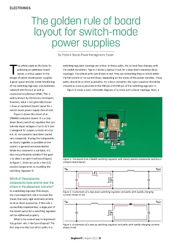
Figure 1 shows the circuit of an
LT8640S evaluation board. It is a step-
down (buck) switching regulator that can
tolerate input voltages of up to 42 V and
is designed for output currents of up to
6 A. All components have been placed
very compactly. Placing the components
as closely together as possible on the
board is a general recommendation.
While this statement is not false, it is
also not particularly suitable if the goal
is to obtain an optimised board layout. Figure 1: The board of an LT8640S switching regulator with closely spaced components and thus a
In Figure 1, there are quite a few (11) compact board layout.
passive components surrounding the
switching regulator IC.
Which of these passive
components have priority over the
others in the placement and why?
In a switching regulator PCB design, Figure 2. A schematic of a step-down switching regulator and paths with rapidly changing
the most important rule is to route the currents shown in red.
traces that carry high switched currents
to be as short as possible. If this rule is
successfully implemented, a large part of
the board layout for a switching regulator
will be addressed properly.
What is the easiest way to implement
this golden rule in the board layout? The Figure 3. A schematic of a step-up switching regulator and paths with rapidly changing currents
first step is to find out which paths in a shown in red.
EngineerIT | August 2022 | 18