Page 24 - EngineerIT August 2022 Digital
P. 24
INDUSTRY 4.0


                                                               transients, reduces noise from ground loops, and creates
                                                               physical safety.
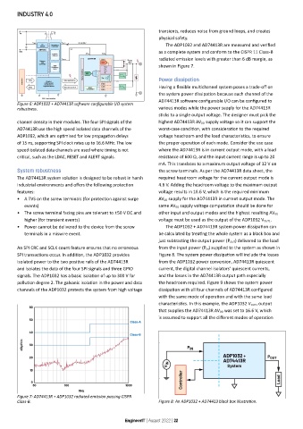
                                                                  The ADP1032 and AD74413R are measured and verified
                                                               as a complete system and conform to the CISPR 11 Class-B
                                                               radiated emission levels with greater than 6 dB margin, as
                                                               shown in Figure 7.


                                                               Power dissipation
                                                               Having a flexible multichannel system poses a trade-off on
                                                               the system power dissipation because each channel of the
                                                               AD74413R software configurable I/O can be configured to
        Figure 6: ADP1032 + AD74413R software configurable I/O system
        robustness.                                            various modes while the power supply for the AD74413R
                                                               sticks to a single output voltage. The designer must pick the
        channel density in their modules. The four SPI signals of the   highest AD74413R AV DD supply voltage so it can support the
        AD74413R use the high speed isolated data channels of the   worst-case condition, with consideration to the required
        ADP1032, which are optimised for low propagation delays   voltage headroom and the load characteristics, to ensure
        of 15 ns, supporting SPI clock rates up to 16.6 MHz. The low   the proper operation of each mode. Consider the use case
        speed isolated data channels are used where timing is not   where the AD74413R is in current output mode, with a load
        critical, such as the LDAC, RESET and ALERT signals.   resistance of 600 Ω, and the input current range is up to 20
                                                               mA. This translates to a maximum output voltage of 12 V on
        System robustness                                      the screw terminals. As per the AD74413R data sheet, the
        The AD74413R system solution is designed to be robust in harsh   required headroom voltage for the current output mode is
        industrial environments and offers the following protection   4.6 V. Adding the headroom voltage to the maximum output
        features:                                              voltage results in 16.6 V, which is the required minimum
        •  A TVS on the screw terminals (for protection against surge   AV DD supply for the AD74413R in current output mode. The
           events)                                             same AV DD supply voltage computation should be done for
        •  The screw terminal facing pins are tolerant to ±50 V DC and   other input and output modes and the highest resulting AV DD
           higher (for transient events)                       voltage must be used as the output of the ADP1032 V OUT1.
        •  Power cannot be delivered to the device from the screw   The ADP1032 + AD74413R system power dissipation can
           terminals in a miswire event.                       be calculated by treating the whole system as a black box and
                                                               just subtracting the output power (P OUT) delivered to the load
        An SPI CRC and SCLK count feature ensures that no erroneous   from the input power (P IN) supplied to the system as shown in
        SPI transactions occur. In addition, the ADP1032 provides   Figure 8. The system power dissipation will include the losses
        isolated power to the two positive rails of the AD74413R   from the ADP1032 power conversion, AD74413R quiescent
        and isolates the data of the four SPI signals and three GPIO   current, the digital channel isolators’ quiescent currents,
        signals. The ADP1032 has a basic isolation of up to 300 V for   and the losses in the AD74413R output path especially
        pollution degree 2. The galvanic isolation in the power and data   the headroom required. Figure 9 shows the system power
        channels of the ADP1032 protects the system from high voltage   dissipation with all four channels of AD74413R configured
                                                               with the same mode of operation and with the same load
                                                               characteristics. In this example, the ADP1032 V OUT1 output
                                                               that supplies the AD74413R AV DD was set to 16.6 V, which
                                                               is assumed to support all the different modes of operation


        Figure 7: AD74413R + ADP1032 radiated emission passing CISPR
        Class-B.                                               Figure 8: An ADP1032 + AD74413 black box illustration.


                                                  EngineerIT | August 2022 | 22

