Page 25 - EngineerIT January 2022
P. 25
ICT – RADIO COMMUNICATION


                                                               Figure 11: Example of wet solder paste (prior to reflow) on a copper ground
                                                               pad that has been deposited by a solder stencil with multiple smaller
                                                               apertures for the ground pad. Signal pins are shown at the top of the
                                                               picture for reference.
        Figure 9: ADAR1000 solder mask with 0.3 mm × 0.3 mm pad openings and
        3.378 mm × 4.369 mm ground paddle opening.
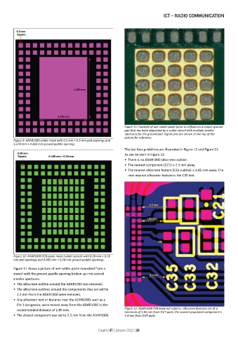
                                                               The last four guidelines are illustrated in Figure 12 and Figure 13.
                                                               As can be seen in Figure 12:
                                                               •  There is no ADAR1000 silkscreen outline.
                                                               •  The nearest component (C21) is 2.3 mm away.
                                                               •  The nearest silkscreen feature (C21 outline) is 1.85 mm away. The
                                                                 next nearest silkscreen feature is the C35 text.

                                                               Shown in Figure 13, both the DUT silkscreen text and the Pin 1


        Figure 10: ADAR1000 PCB paste mask (solder stencil) with 0.28 mm × 0.28
        mm pad openings and 0.406 mm × 0.28 mm ground paddle openings.

        Figure 11 shows a picture of wet solder paste deposited from a
        stencil with the ground paddle opening broken up into several
        smaller apertures.
        •  The silkscreen outline around the ADAR1000 was removed.
        •  The silkscreen outlines around the components that are within
          2.3 mm from the ADAR1000 were removed.
        •  Any silkscreen text or features near the ADAR1000, such as a
          Pin 1 designator, were moved away from the ADAR1000 to the
          recommended distance of 1.85 mm.                     Figure 12: ADAR1000 PCB keep-out regions; silkscreen features are at a
                                                               minimum of 1.85 mm from DUT pads; the nearest populated component is
        •  The closest component was set to 2.3 mm from the ADAR1000.  2.3 mm from DUT pads.


                                                  EngineerIT | January 2022 | 23

