Page 22 - EngineerIT January 2022
P. 22
ICT – RADIO COMMUNICATION


        Reliable PCB assembly of land grid


        array packages in planar phased


        array antennas


        By Joel Dobler, Staff Product Applications Engineer, and Eamon Nash, Applications Director


             igh frequency planar phased arrays often require a
             complexity from their beam-forming ICs and transmit/
       Hreceive (T/R) modules that force the devices into high pin
        count land grid array (LGA) packages, so that all the RF circuits fit
        into a λ/2 lattice spacing. LGA packages have recessed pins located
        on their bottom side. As a result, PCB solder mask variation and
        solder volume invariance both contribute to difficult PCB assembly
        if the LGA footprint is not designed correctly. This article gives
        guidelines for proper LGA footprint design that leads to high yield
        PCB assembly and gives a practical LGA footprint design example
        using the large, high pin count ADAR1000 beamformer IC.

        Planar phased array systems
        Phased array technology uses an arrangement of antenna elements
        where the relative phase of each element is varied to steer the
        focused radiation pattern, also known as a beam. The beam can be
        aimed in various directions electronically, overcoming the limited
        speed and reliability problems of a mechanically steered antenna.
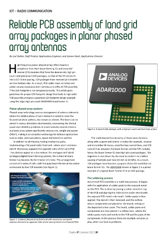
        A phased array system significantly reduces size, weight and power   Figure 2: A typical LGA package, with a high pin count and dual rings of pins.
        (SWaP), making it an attractive technology for defence applications
        such as radar, communications, space and electronic warfare.  The multichannel functionality of these beam formers,
           In addition to eliminating moving mechanical parts,   along with support and control circuitry (for example, receiver
        implementing a flat panel radar front end - where patch antennas   and transmitter RF traces, amplifier bias control lines, and T/R
        and RF electronics populate the opposite sides of the same PCB   control lines between the beam former and the T/R module)
        - has obvious appeal as a size reducer. For analogue and hybrid   forces the beam former ICs into high pin count packages. This
        (analogue/digital) beam forming systems, the 4-channel beam   migration is also driven by the need to conform to a lattice
        former has become the form factor of choice. This arrangement   spacing of lambda over two (15 mm at 10 GHz). As a result,
        consists of a series of cells, with the quad beam former at the centre   LGA packages have become a popular choice for multichannel
        surrounded by four T/R modules (see Figure 1).         beam former ICs. The ADAR1000 shown in Figure 2 is a prime
                                                               example of a typical beam former IC in an LGA package.

                                                               The soldering process
                                                               Automated PCB assembly is a multi-step process. It begins
                                                               with the application of solder paste to the exposed metal
                                                               on the PCB. This is done by placing a solder stencil on top
                                                               of the PCB and aligning the holes in the solder stencil with
                                                               the exposed PCB metal underneath. Solder paste is then
                                                               applied. The stencil is then removed, and the surface-
                                                               mount components are placed on the board, resting on
                                                               the deposited solder paste. The board, solder paste and
                                                               components are then placed in a reflow oven, where the
                                                               solder paste melts and bonds to the PCB and the pads of the
                                                               components. In this process there are multiple variables at
        Figure 1: A planar phased array front end with electronics and patch
        antenna elements on opposite sides of the same printed circuit board (PCB).  play, which can lead to problems.


                                                  EngineerIT | January 2022 | 20

