Page 23 - EngineerIT January 2022
P. 23
ICT – RADIO COMMUNICATION


        Solder mask variance and stencil invariance
        Along with the solder stencil, the solder mask on the PCB (which
        usually has a familiar green colour) defines where solder paste
        should be applied to the PCB. A popular design approach involves
        making the solder mask openings (apertures) slightly smaller than
        the metal pads underneath (so-called solder mask defined pads).
           Many PCBs use liquid photo-imageable (LPI) solder masks
        that meet the IPC-SM-840 Class 3 standard. Depending on the
        fabrication lot, vendor, etc., the solder mask apertures can vary in
        size and be misaligned due to solder mask registration errors. An
        example of a solder mask with varying apertures is shown in Figure
        3 (highlighted with red rectangles).


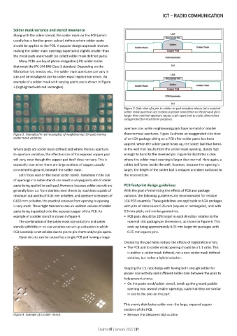
                                                               Figure 5: Side view of a pin-to-solder-to-pad interface where (a) a nominal
                                                               solder mask aperture size creates a proper connection to the pin and (b) a
                                                               larger than nominal aperture causes a pin open (not to scale; dimensions
                                                               exaggerated for illustration purpose).

                                                               aperture size, while neighbouring pads have nominal or smaller
        Figure 3: Examples (in red rectangles) of neighbouring LGA pads having   than nominal apertures. Figure 5a shows an exaggerated side view
        solder mask variation.                                 of an LGA package sitting on a PCB after solder paste has been
                                                               applied. When the solder paste heats up, the solder ball that forms
        Where pads are solder mask defined and where there is aperture-  in the well that results from the solder mask opening, stands high
        to-aperture variation, the effective size of the exposed copper pad   enough to bond to the recessed pin. Figure 5b illustrates a case
        will vary, even though the copper pad itself does not vary. This is   where the solder mask opening is larger than normal. Here again, a
        especially true when there are large sections of copper, usually   solder ball forms inside the well. However, because the opening is
        connected to ground, beneath the solder mask.          larger, the height of the solder ball is reduced and does not bond to
           Let’s focus next on the metal solder stencil. Variations in the size   the recessed pin.
        of openings in a solder stencil can result in varying amounts of solder
        paste being applied to each pad. However, because solder stencils are   PCB footprint design guidelines
        generally laser cut from stainless steel sheets by machines capable of   With the goal of minimising the effects of PCB and package
        minimum cut widths of 0.05 mm or better, and aperture tolerances of   variance, the following guidelines are recommended for reliable
        0.013 mm or better, the practical variance from opening to opening   LGA PCB assembly. These guidelines are applicable to LGA packages
        is very small. These tight tolerances ensure uniform volume of solder   with pins of dimensions 0.25 mm (square or rectangular), and with
        paste being deposited onto the exposed copper of the PCB. An   0.5 mm pitch, and similar geometries.
        example of a solder stencil is shown in Figure 4.      •  PCB pads should be 20% larger in each direction relative to the
           The combination of the solder mask size variations and solder   nominal LGA package pin dimensions, as shown in Figure 6. This
        stencils with little or no size variation can set up a situation in which   ends up being approximately 0.05 mm larger for packages with
        PCB assembly is not reliable due to pin-to-pin shorts and/or pin opens.  0.25 mm square pins.
           Open circuits can be caused by a single PCB pad having a larger
                                                               Oversizing the pad helps reduce the effects of registration errors.
                                                               •  The PCB pad to solder mask opening should be a 1:1 ratio. This
                                                                 is neither a solder mask defined, nor a non-solder mask defined
                                                                 solution, but rather a hybrid solution.

                                                               Keeping the 1:1 ratio helps with having both enough solder for
                                                               proper connectivity and sufficient solder dam between the pads to
                                                               help prevent shorts.
                                                               •  On the paste mask/solder stencil, break up the ground paddle
                                                                 opening into several smaller openings, such that they are similar
                                                                 in size to the pins on the part.


                                                               This evenly distributes solder over the large, exposed copper
                                                               sections of the PCB.
        Figure 4: Example of a solder stencil.                 •  Remove the silkscreen LGA outline.


                                                  EngineerIT | January 2022 | 21

