Page 26 - EngineerIT January 2022
P. 26
ICT – RADIO COMMUNICATION


                                                               element spacing set to λ/2, successfully soldering them to a PCB
                                                               can be challenging. The main guidelines discussed in this article
                                                               of 1) increasing the PCB pad size by 20% larger than the LGA
                                                               pins, 2) setting the solder mask aperture to be the same size as
                                                               the PCB pads, and 3) designing the solder stencil such that the
                                                               ground paddle opening is broken up into smaller apertures that
                                                               are similar in size to the pins of the LGA, all contribute to reducing
                                                               the effect of PCB manufacturing variances. These guidelines have
                                                               been proven to deliver a high yield board assembly consistently
                                                               across manufacturing and assembly lots. Having reliable assembly
                                                               prevents the need for any PCB rework, which saves money and
                                                               decreases time to market.                       n


                                                               Analog Devices is represented in South Africa by Arrow Altech.
                                                               For more information email Conrad Coetzee at
                                                               ccoetzee@arrow.altech.co.za

                                                               About the authors
                                                               -  Joel Dobler is a staff product applications engineer in the
                                                                 Aerospace and Defense Group, focusing on beam former
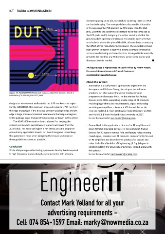
        Figure 13: ADAR1000 PCB keep-out regions; silkscreen features are at a   products, but also supporting vector modulators and
        minimum of 1.85 mm from DUT pads.
                                                                 programmable low-pass filters. He has worked for Analog
                                                                 Devices since 2006, supporting a wide range of RF products
        designator were moved well outside the 1.85 mm keep-out region.   including logarithmic and rms detectors, digital and analog
        For the ADAR1000, this minimum keep-out region is 1.795 mm from   variable gain amplifiers, mixers and I/Q demodulators. He
        the edge of package. If the distance between package edge and pin   received his B.S.E.E. from Washington State University in 2005
        edge is large, it is recommended to reference the keep-out regions   and his M.E.E.E from Portland State University in 2007.
        to the package edge, instead of the pin edge as shown in this article.    He can be reached at joel.dobler@analog.com.
           The ADAR1000 evaluation board allowed for keeping the
        nearest components and silkscreen features well away from the   -  Eamon Nash is the applications director for RF amplifiers and
        ADAR1000. This keep-out region is not always possible on planar   beam formers at Analog Devices. He has worked at Analog
        phased array application boards, but board designers should keep   Devices for 30 years in various field and factory roles covering
        this guideline in mind when designing their board and observe   mixed-signal, precision and RF products. He is currently focused
        these guidelines as best as possible.                    on RF amplifiers and beam former products for satcom and
                                                                 radar. He holds a Bachelor of Engineering (B.Eng.) degree in
        Conclusion                                               electronics from the University of Limerick, Ireland, along with
        While LGA packages offer the high pin count density that is required   five patents.
        in high frequency planar phased array electronics with antenna     He can be reached at eamon.nash@analog.com.


                              Contact Mark Yelland for all your


                                   advertising requirements -


             Cell: 074 854-1597 Email: marky@nowmedia.co.za

