Page 19 - EngineerIT October 2022
P. 19
ELECTRONICS


           In general, high performance data collecting systems
        should have four or more layers. The top layer is often used
        for digital/analogue signals, while the bottom layer is used
        for auxiliary signals. The second layer (ground layer) serves
        as a reference plane for impedance-controlled signals and is
        used for reducing IR drops and shielding the digital signals in
        the top layer. Finally, the power plane is on the third layer.
           Power and ground planes must be adjacent to each other
        as they provide additional interplane capacitance, which
        helps with the high frequency decoupling of the power
        supply.
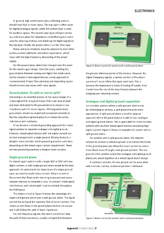
           For the ground layer, advice has changed over the years   Figure 4: Return current for system with a solid ground plane.
        for the mixed-signal design. Over the years, splitting the
        ground plane between analog and digital has made sense   the ground reference points of the devices. However, for
        but for modern mixed-signal devices, a new approach is   higher frequency signals, a certain portion of the return
        recommended. Proper floor planning and separating signals   current will try to follow the signal path back. This is
        should prevent any issues with noisy signals.          because the impedance is lower following this path, since
                                                               it minimises the size of the loop formed between the
        Ground plane: To split or not to split?                outgoing and returning current.
        Grounding is an essential process in the layout design of a
        mixed-signal PCB. A typical 4-layer PCB must have at least   Analogue and digital ground separation
        one layer dedicated to the ground plane to ensure a low   For complex systems where a solid ground scheme can
        impedance path for return signals. All integrated circuit   be challenging to achieve, a split ground may be more
        ground pins should be routed and connected correctly to   appropriate. A split ground plane is another popular
        the low impedance ground plane to minimise the series   approach where the ground plane is split in two: analogue
        inductance and resistance.                             and digital ground planes. This is applicable for more complex
           It has become a standard grounding approach for mixed-  systems with multiple mixed-signal devices consuming high
        signal systems to separate analogue and digital ground.   digital current. Figure 5 shows an example of a system with a
        However, mixed-signal devices with low digital current can   split ground plane.
        be best managed with a single ground. Moving forward, a   For systems with a split ground plane, the simplest
        designer must consider which grounding practice suits best,   solution to achieve a cohesive ground is to remove the break
        depending on the mixed-signal current requirement. There   in the ground planes and allow the return current to take a
        are two grounding practices a designer must consider.  more direct route through a star ground junction. The star
                                                               ground is the junction where the analogue and digital ground
        Single ground plane                                    planes are joined together on a mixed-signal layout design.
        For mixed-signal systems with a single ADC or DAC with low   In common systems, the star ground can be associated
        digital current, a solid single ground plane would be the best   with a simple, narrow, continued junction in between
        approach. To understand the importance of a single ground
        layer, we need to recall return current. Return current is
        the current that flows while returning to ground and traces
        between devices to complete a loop. To prevent mixed-signal
        interference, each return path must be tracked throughout
        the PCB layout.
           The simple circuit in Figure 4 shows the advantage of a
        single solid ground plane over a split ground plane. The signal
        current has an equal but opposite flow of return current. This
        return current flows in the ground plane back to the source
        and it will follow the path of least impedance.
           For low frequency signals, the return current will take
        the path of least resistance, usually a straight line between   Figure 5: Return current for systems with a split ground plane.


                                                  EngineerIT | October 2022 | 17

