Page 16 - EngineerIT October 2022
P. 16
ELECTRONICS


          Basic guidelines for layout  design


                             of mixed-signal PCBs


                    By May Anne Porley, applications engineer, and Kevin Chesser, product application engineer


             his article will detail what to consider when designing   the board, while auxiliary components such as decoupling
             the layout of mixed-signal PCBs. It covers component   capacitors and crystals must be placed as close as possible to
        Tplacement, board layering and ground plane            the mixed-signal device.
        considerations. The guidelines discussed in this article provide
        a practical approach to the layout design of mixed-signal boards   Analogue and digital blocks partition
        and should assist engineers of all backgrounds.        To help minimise the common return path for analogue and
                                                               digital signals, analogue and digital block separation may be
        Introduction                                           considered, such that analogue signals will not mix with digital
        A mixed-signal PCB design requires basic understanding of   signals.
        analogue and digital circuitry to minimise, if not prevent, signal
        interference. Modern systems consist of components that
        are operational with both digital and analogue domains, and
        these must be carefully designed to ensure signal integrity all
        throughout the system.
           PCB layout, as an important part of the mixed-signal
        development process, can be intimidating and component
        placement is just the beginning. There are also other factors
        that must be considered, including board layers and how to
        properly manage these to minimise interferences caused by
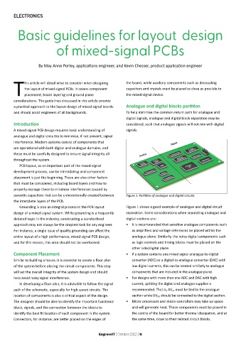
        parasitic capacitors that can be unintentionally created between   Figure 1: Partition of analogue and digital circuits.
        the interplane layers of the PCB.
           Grounding is also an integral process in the PCB layout   Figure 1 shows a good example of analogue and digital circuit
        design of a mixed-signal system. While grounding is a frequently   separation. Some considerations when separating analogue and
        debated topic in the industry, constructing a standardised   digital sections are:
        approach may not always be the simplest task for any engineer.   •  It is recommended that sensitive analogue components such
        For instance, a single issue of quality grounding can affect the   as amplifiers and voltage references be placed within the
        entire layout of a high performance, mixed-signal PCB design,   analogue plane. Similarly, the noisy digital components such
        and for this reason, this area should not be overlooked.  as logic controls and timing blocks must be placed on the
                                                                  other side/digital plane.
        Component Placement                                    •  If a system contains one mixed-signal analogue-to-digital

        Similar to building a house, it is essential to create a floor plan   converter (ADC) or a digital-to-analogue converter (DAC) with
        of the system before placing the circuit components. This step   low digital currents, this can be treated similarly to analogue
        will set the overall integrity of the system design and should   components that are included in the analogue plane.
        help avoid noisy signal interference.                  •  For designs with more than one ADC and DAC with high
           In developing a floor plan, it is advisable to follow the signal   current, splitting the digital and analogue supplies is
        path of the schematic, especially for high-speed circuits. The   recommended. That is, AV CC must be tied to the analogue
        location of components is also a critical aspect of the design.   section while DV DD should be connected to the digital section.
        The designer should be able to identify the important functional   •  Micro-processors and micro-controllers may take up space
        block, signals, and the connection between the blocks to   and will generate heat. These components must be placed in
        identify the best fit location of each component in the system.   the centre of the board for better thermal dissipation, and at
        Connectors, for instance, are better placed on the edges of   the same time, close to their related circuit blocks.


                                                  EngineerIT | October 2022 | 14

