Page 38 - EngineerIT June 2022
P. 38
INDUSTRY, TECHNOLOGY, PRODUCTS AND INNOVATION


           A new age of 2.5D materials: important


           development for high performance


           rechargeable batteries


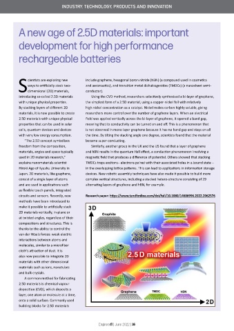
               cientists are exploring new   include graphene, hexagonal boron nitride (hBN) (a compound used in cosmetics
               ways to artificially stack two-  and aeronautics), and transition metal dichalcogenides (TMDCs) (a nanosheet semi-
          Sdimensional (2D) materials,       conductor).
           introducing so-called 2.5D materials   Using the CVD method, researchers selectively synthesised a bi-layer of graphene,
           with unique physical properties.   the simplest form of a 2.5D material, using a copper-nickel foil with relatively
           By stacking layers of different 2D   high nickel concentration as a catalyst. Nickel makes carbon highly soluble, giving
           materials, it is now possible to create   researchers more control over the number of graphene layers. When an electrical
           2.5D materials with unique physical   field was applied vertically across the bi-layer of graphene, it opened a band gap,
           properties that can be used in solar   meaning that its conductivity can be turned on and off. This is a phenomenon that
           cells, quantum devices and devices   is not observed in mono layer graphene because it has no band gap and stays on all
           with very low energy consumption.   the time. By tilting the stacking angle one degree, scientists found that the material
             “The 2.5D concept symbolises    became super-conducting.
           freedom from the composition,       Similarly, another group in the UK and the US found that a layer of graphene
           materials, angles and space typically   and hBN results in the quantum Hall effect, a conduction phenomenon involving a
           used in 2D materials research,”   magnetic field that produces a difference of potential. Others showed that stacking
           explains nanomaterials scientist   TMDCs traps excitons– electrons paired with their associated holes in a bound state ¬
           Hiroki Ago of Kyushu University in   in the overlapping lattice patterns. This can lead to applications in information storage
           Japan. 2D materials, like graphene,   devices. New robotic assembly techniques have also made it possible to build more
           consist of a single layer of atoms   complex vertical structures, including a stacked hetero-structure consisting of 29
           and are used in applications such   alternating layers of graphene and hBN, for example.
           as flexible touch panels, integrated
           circuits and sensors. Recently, new   Research paper: https://www.tandfonline.com/doi/full/10.1080/14686996.2022.2062576
           methods have been introduced to
           make it possible to artificially stack
           2D materials vertically, in-plane or
           at twisted angles, regardless of their
           compositions and structures. This is
           thanks to the ability to control the
           van der Waals forces: weak electric
           interactions between atoms and
           molecules, similar to a microfiber
           cloth’s attraction of dust. It is
           also now possible to integrate 2D
           materials with other dimensional
           materials such as ions, nanotubes
           and bulk crystals.
             A common method for fabricating
           2.5D materials is chemical vapour
           deposition (CVD), which deposits a
           layer, one atom or molecule at a time,
           onto a solid surface. Commonly used
           building blocks for 2.5D materials


                                                   EngineerIT | June 2022 | 36

