
Page 15 - EngineerIT April 2022
P. 15
ICT COMMUNICATION
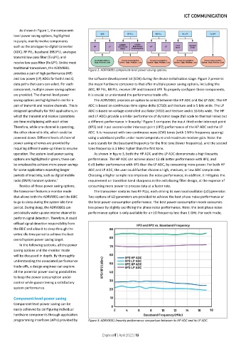
As shown in Figure 1, the component-
level power saving options, highlighted
in purple, mainly involve components
such as the analogue-to-digital converter
(ADC), RF PLL, baseband (BB) PLL, analogue
transmit low-pass filter (Tx LPF), and
receive low-pass filter (Rx LPF). Unlike most
traditional transceivers, the ADRV9001 Figure 2: ADRV9001 component-level power saving options.
provides a pair of high performance (HP)
and low power (LP) ADCs for both I and Q the software development kit (SDK) during the device initialisation stage. Figure 2 presents
data paths that users can select. For each the major hardware components that offer multiple power saving options, including the
component, multiple power saving options ADC, RF PLL, BB PLL, receive LPF and transmit LPF. To properly configure those components,
are provided. The channel-level power it is crucial to understand the performance trade-offs.
saving options are highlighted in red for a The ADRV9001 provides an option to select between the HP ADC and the LP ADC. The HP
pair of transmit and receive channels. This is ADC is based on continuous-time sigma-delta (CTSD) architecture and is 5 bits wide. The LP
designed specifically for TDD applications, in ADC is based on voltage-controlled oscillator (VCO) architecture and is 16 bits wide. The HP
which the transmit and receive operations and LP ADCs provide a similar performance of dynamic range (full scale to thermal noise) but
are time multiplexing with each other. a different performance in linearity. Figure 3 compares the input third-order intercept point
2
Therefore, while one channel is operating, (IIP3) and input second-order intercept point (IIP2) performance of the HP ADC and the LP
the other channel is idle, which could be ADC. It is measured with two continuous wave (CW) tones (with 1 MHz frequency spacing)
powered down. Different levels of channel using a wideband profile under room temperature and maximum receiver gain. Note: the
power saving schemes are provided by x-axis stands for the baseband frequency for the first tone (lower frequency), and the second
requiring different wake-up times to resume tone frequency is 1 MHz higher than the first tone.
operation. The system-level power saving As shown in figure 3, both the HP ADC and the LP ADC demonstrate a high linearity
options are highlighted in green; these can performance. The HP ADC can achieve about 12 dB better performance with IIP2, and
be employed to achieve more power savings 6 dB better performance with IIP3 than the LP ADC, by consuming more power. For both HP
for some applications expecting longer ADC and LP ADC, the user could further choose a high, medium, or low ADC sample rate.
periods of inactivity, such as digital mobile Choosing a higher sample rate improves the noise performance; in addition, it mitigates the
radio (DMR) handset systems. 1 requirement on transition band sharpness in the antialiasing filter design, at the expense of
Besides all those power saving options, consuming more power to process data at a faster rate.
the transceiver features a monitor mode The transceiver contains two RF PLLs, each driving its own local oscillator (LO) generator.
that allows both the ADRV9001 and the BBIC Two options of LO generators are provided to achieve the best phase noise performance or
to go to sleep during the system idle time the best power consumption performance. The best power consumption mode consumes
period. During sleep, the ADRV9001 can less power by slightly sacrificing the phase noise performance. Note: the best phase noise
periodically wake up one receive channel to performance option is only available for an LO frequency less than 1 GHz. For each mode,
perform signal detection. Therefore, it could
offload signal detection responsibility from
the BBIC and allow it to sleep through the
entire idle time period to achieve the best
overall system power saving target.
In the following sections, all the power
saving options and the monitor mode
will be discussed in depth. By thoroughly
understanding the associated performance
trade-offs, a design engineer can explore
all the potential power saving possibilities
to keep the power consumption under
control while guaranteeing a satisfactory
system performance.
Component-level power saving
Component-level power saving can be
easily achieved by configuring individual
hardware components through application
programming interfaces (APIs) provided by Figure 3: ADRV9001 linearity performance comparison between its HP ADC and its LP ADC.
EngineerIT | April 2022 | 13