Page 18 - EngineerIT April 2022
P. 18
ICT COMMUNICATION


        trigger the power-up and power-down.
        The wake-up time is short—around 4.5 μs.
        The channel power saving Mode 1 further
        powers down the channel’s internal PLL.
        When the PLL is powering up, recalibration is
        mandatory, so the PLL wake-up time includes
        PLL power-up time and PLL calibration time.
        The ADRV9001 provides two PLL calibration
        modes: normal mode and fast mode. The
        fast mode does not guarantee a lock over
        the entire temperature range as the normal
        mode does, but it is more suitable when the
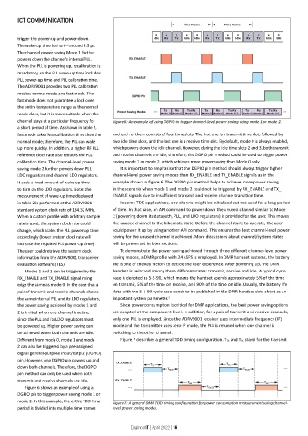
        channel stays at a particular frequency for   Figure 6: An example of using DGPIO to trigger channel-level power saving using mode 1 or mode 2.
        a short period of time. As shown in table 2,
        fast mode takes less calibration time than the   and each of them consists of four time slots. The first one is a transmit time slot, followed by
        normal mode; therefore, the PLL can wake   two idle time slots, and the last one is a receive time slot. By default, mode 0 is always enabled,
        up more quickly. In addition, a higher RF PLL   which powers down the idle channel. However, during the idle time slots 2 and 3, both transmit
        reference clock rate also reduces the PLL   and receive channels are idle; therefore, the DGPIO pin method could be used to trigger power
        calibration time. The channel-level power   saving mode 1 or mode 2, which achieves more power saving than Mode 0 only.
        saving mode 2 further powers down PLL   It is important to emphasise that the DGPIO pin method should always trigger higher
        LDO regulators and channel LDO regulators.   channel-level power saving modes than RX_ENABLE and TX_ENABLE signals as in the
        It adds a fixed amount of wake-up time   example shown in figure 6. The DGPIO pin method helps to achieve more power saving
        to turn on the LDO regulators. Note: the   in the scenario when mode 1 and mode 2 could not be triggered by RX_ENABLE and TX_
        measurement of wake-up time displayed   ENABLE signals due to insufficient transmit and receive channel transition time.
        in table 2 is performed at the ADRV9001   In some TDD applications, one channel might be initialised but not used for a long period
        standard system clock rate of 184.32 MHz.   of time. In that case, an API command to power down the unused channel similar to Mode
        When a custom profile with arbitrary sample   2 (powering down its datapath, PLL, and LDO regulators) is provided for the user. This moves
        rate is used, the system clock rate could   the unused channel to the hibernate state. Before the channel starts to operate, the user
        change, which scales the PLL power-up time   could power it up by using another API command. This ensures the best channel-level power
        accordingly (lower system clock rate will   saving for the unused channel is achieved. More discussions about channel/system states
        increase the required PLL power-up time).   will be presented in later sections.
        The user could retrieve the system clock   To demonstrate the power saving achieved through three different channel-level power
        information from the ADRV9001 transceiver   saving modes, a DMR profile with 24 kSPS is employed. In DMR handset systems, the battery
        evaluation software (TES).           life is one of the key factors to decide the user experience. After powering up, the DMR
           Modes 1 and 2 can be triggered by the   handset is switched among three different states: transmit, receive and idle. A typical cycle
        RX_ENABLE and TX_ENABLE signal rising   case is denoted as 5-5-90, which means the handset spends approximately 5% of the time
        edge the same as mode 0. In the case that a   on transmit, 5% of the time on receive, and 90% of the time on idle. Usually, the battery life
        pair of transmit and receive channels shares   data with the 5-5-90 cycle case needs to be published in the DMR handset data sheet as an
        the same internal PLL and its LDO regulators,   important system parameter. 1
        the power saving achieved by modes 1 and   Since power consumption is critical for DMR applications, the best power saving options
        2 is limited when one channel is active,   are adopted at the component level. In addition, for a pair of transmit and receive channels,
        since the PLL and its LDO regulators must   only one PLL is employed. Since the ADRV9001 receiver uses intermediate frequency (IF)
        be powered up. Higher power saving can   mode and the transmitter uses zero-IF mode, the PLL is retuned when one channel is
        be achieved when both channels are idle.   switching to the other channel.
        Different from mode 0, mode 1 and mode   Figure 7 describes a general TDD timing configuration. T TX and T RX stand for the transmit
        2 can also be triggered by a pre-assigned
        digital general-purpose input/output (DGPIO)
        pin. However, one DGPIO pin powers up and
        down both channels. Therefore, the DGPIO
        pin method can only be used when both
        transmit and receive channels are idle.
           Figure 6 shows an example of using a
        DGPIO pin to trigger power saving mode 1 or
        mode 2. In this example, the entire TDD time   Figure 7: A general DMR TDD timing configuration for power consumption measurement using channel-
        period is divided into multiple time frames   level power saving modes.


                                                    EngineerIT | April 2022 | 16

