Page 19 - EngineerIT April 2022
P. 19
ICT COMMUNICATION


        and receive active time, respectively. T IDLE1 and T IDLE2 stand for the idle time. For simplicity,   System-level power saving
        wake-up time is not indicated since in general it is much shorter compared with the channel   As discussed in the previous section,
        active and idle time; therefore, it is insignificant in power consumption calculation.  channel-level power saving modes power
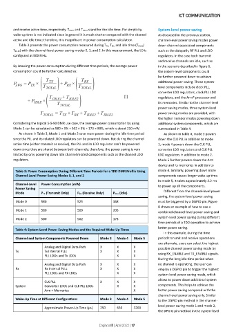
           Table 3 presents the power consumption measured during T TX, T RX, and idle time (T IDLE1/  down channel-associated components
        T IDLE2) with the channel-level power saving modes 0, 1, and 2. In this measurement, the LO is   such as the datapath, RF PLL and LDO
        configured at 900 MHz.                                                    regulators. In the case both transmit
                                                                                  and receive channels are idle, such as
        By knowing the power consumption during different time periods, the average power   in the scenario described in figure 6,
        consumption could be further calculated as:                               the system-level components could
                                                                                  be further powered down to achieve
                                                                                  additional power saving. Those system-
                                                                                  level components include clock PLL,
                                                                                  converter LDO regulators, clock PLL LDO
                                                                                  regulators, and the Arm® processor and
                                                                                  its memories. Similar to the channel-level
                                                                                  power saving modes, three system-level
                                                                                  power saving modes are provided, with
                                                                                  the higher number modes powering down
        Considering the typical 5-5-90 DMR use case, the average power consumption by using   additional system components, which are
        Mode 2 can be calculated as 580 × 5% + 502 × 5% + 173 × 90%, which is about 210 mW.  summarized in Table 4.
           As shown in Table 3, Mode 1 and Mode 2 save more power during the idle time period   As shown in table 4, mode 3 powers
        since the PLL and its related LDO regulators can be powered down. But during the channel   down the CLK PLL in addition to mode
        active time (either transmit or receive), the PLL and its LDO regulator can’t be powered   1, mode 4 powers down the CLK PLL,
        down since they are shared between both channels; therefore, the power saving is very   converter LDO regulators and CLK PLL
        limited by only powering down idle channel related components such as the channel LDO   LDO regulators in addition to mode 2.
        regulators.                                                               Mode 5 further powers down the Arm
                                                                                  device and its memories in addition to
         Table 3: Power Consumption During Different Time Periods for a TDD DMR Profile Using   mode 4. Similarly, powering down more
         Channel-Level Power Saving Modes 0, 1, and 2                             components causes longer wake-up time.
                                                                                  In mode 5, it takes approximately 3.2 ms
         Channel-Level   Power Consumption (mW)                                   to power up all the components.
         Power Saving
         Mode         P TX (Transmit Only)   P RX (Receive Only)   P IDLE (Idle)    Different from the channel-level power
                                                                                  saving, the system-level power saving
         Mode 0       580               525                368                    must be triggered by a DGPIO pin. Figure
                                                                                  8 shows an example of how to use a
         Mode 1       580               509                205                    combined channel-level power saving and

         Mode 2       580               502                173                    system-level power saving during different
                                                                                  time periods of a TDD operation to achieve
                                                                                  better power saving.
         Table 4: System-Level Power Saving Modes and the Required Wake-Up Times
                                                                                    In this example, during the time
         Channel and System Components Powered Down   Mode 3   Mode 4   Mode 5    period transmit and receive operations
                                                                                  are alternate, users can select the highest
                        Analog and Digital Data Path   X     X       X            possible channel power saving mode by
         Tx             Tx Internal PLLs            X        X       X
                        PLL LDOs and Tx LDOs                 X       X            using RX_ENABLE and TX_ENABLE signals.
                                                                                  During the long idle time period when
                        Analog and Digital Data Path   X     X       X            no channel is operating, the user can
         Rx             Rx Internal PLLs            X        X       X            employ a DGPIO pin to trigger the highest
                        PLL LDOs and RX LDOs                 X       X            system-level power saving mode, which
                                                                                  allows to power down additional system
                        CLK PLL                     X        X       X
         System         Converter LDOs and CLK PLL LDOs      X       X            components. This helps to achieve the
                        Arm + Memories                               X            better power saving compared with the
                                                                                  channel-level power saving only. Similar
         Wake-Up Time at Different Configurations   Mode 3   Mode 4   Mode 5      to the DGPIO pin method in the channel-
                                                                                  level power saving mode 1 and mode 2,
                        Approximate Power-Up Time (µs)   250   650   3200
                                                                                  the DPGIO pin method in the system-level


                                                    EngineerIT | April 2022 | 17

